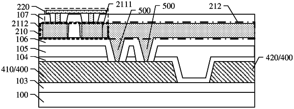
| CPC H01L 27/156 (2013.01) [H01L 33/387 (2013.01); H01L 33/62 (2013.01)] | 18 Claims |

|
1. A light emitting plate, comprising:
a base substrate; and
a plurality of light emitting units, arranged on the base substrate along a first direction and a second direction, each of the plurality of light emitting units comprising at least one light emitting sub-unit, the light emitting sub-unit comprising a connection line unit and a light emitting diode chip connected with the connection line unit, the light emitting diode chip being located at a side of the connection line unit away from the base substrate;
wherein each connection line unit comprises at least two electrical contact pairs, and each of the at least two electrical contact pairs comprises a first electrode contact and a second electrode contact; in each connection line unit, the first electrode contacts are electrically connected with each other, the second electrode contacts are electrically connected with each other, and only one electrical contact pair of the at least two electrical contact pairs is connected with the light emitting diode chip.
|