| CPC H01L 27/14687 (2013.01) [H01L 27/14632 (2013.01)] | 16 Claims |
|
1. A method for manufacturing a sensor device with a buried deep trench structure, the method comprising:
providing a semiconductor substrate having a sensing region which extends vertically below a main surface region of the semiconductor substrate into the semiconductor substrate, wherein a masking layer is arranged on the main surface region of the semiconductor substrate;
etching a deep trench structure into the semiconductor substrate through revealed areas of the masking layer such that the deep trench structure is arranged laterally relative to the sensing region and vertically from the main surface region into the semiconductor substrate;
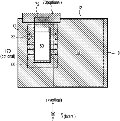
selectively depositing by epitaxy a doped semiconductor layer on a surface region of the deep trench structure to provide a coated deep trench structure;
at least partially removing the masking layer to reveal the main surface region of the semiconductor substrate;
depositing a semiconductor capping layer on the main surface region of the semiconductor substrate, wherein the semiconductor capping layer covers and closes the coated deep trench structure and forms together with the semiconductor substrate a thickened semiconductor substrate having the buried deep trench structure; and
out-diffusing dopants of the doped semiconductor layer into the thickened semiconductor substrate, wherein the out-diffused dopants provide a trench doping region that extends from the doped semiconductor layer into the thickened semiconductor substrate,
wherein depositing the semiconductor capping layer comprises:
depositing a first semiconductor capping layer on the main surface region of the semiconductor substrate; and
depositing a second semiconductor capping layer on the first semiconductor capping layer,
wherein the first semiconductor capping layer and the second semiconductor capping layer together form the semiconductor capping layer, and
wherein the depositing of the first semiconductor capping layer is performed at a lower temperature than the depositing of the second semiconductor capping layer.
|