| CPC H01L 27/14643 (2013.01) [H01L 27/14683 (2013.01)] | 28 Claims |
|
1. An integrated circuit, comprising:
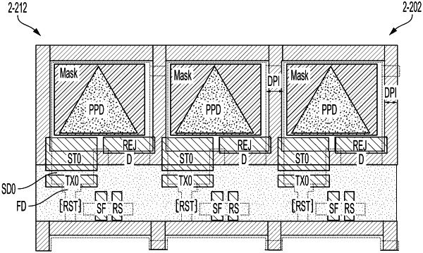
a photodetection region;
a charge storage region electrically coupled to the photodetection region and configured to receive charge carriers from the photodetection region;
a readout region electrically coupled to the charge storage region and configured to receive charge carriers from the charge storage region;
a drain region electrically coupled to the photodetection region and configured to receive charge carriers from the photodetection region and transfer the received charge carriers to a direct current (DC) voltage for draining the charge carriers from the photodetection region; and
an at least partially opaque and at least partially insulative layer disposed above or below at least a portion of the photodetection region, the at least partially opaque and at least partially insulative layer having a triangular-shaped opening configured to receive dopants therethrough,
wherein the photodetection region is configured to induce an intrinsic electric field in a first direction from the photodetection region to the drain region and from the photodetection region to the charge storage region.
|