| CPC H01L 27/14636 (2013.01) [H01L 27/1462 (2013.01); H01L 27/14685 (2013.01); H01L 27/14698 (2013.01)] | 20 Claims |
|
1. A method of fabricating a semiconductor device, comprising:
receiving a device substrate including a pixel region and a bond pad region;
forming a radiation sensor in the pixel region in a front side of the device substrate;
forming an interconnect structure on the front side of the device substrate, the interconnect structure coupled to the radiation sensor;
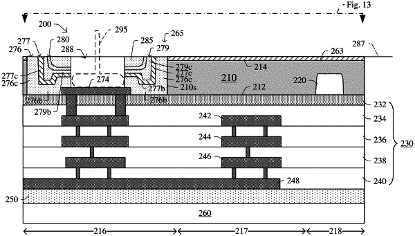
etching a recess into a backside of the device substrate to remove the bond pad region of the device substrate until a portion of the interconnect structure is exposed, wherein the recess has a recess depth and an edge of the recess is defined by a sidewall of the device substrate;
forming a conductive bond pad in the recess, the conductive bond pad coupled to a conductive feature in the interconnect structure;
forming a first plurality of layers covering the conductive bond pad, extending along the sidewall of the device substrate corresponding to the edge of the recess, and covering the backside of the device substrate, wherein each of the first plurality of layers is substantially conformal and wherein the first plurality of layers collectively have a first total thickness that is less than the recess depth; and
performing a first chemical mechanical planarization (CMP) to remove portions of the first plurality of layers from the pixel region so remaining portions of the first plurality of layers cover the conductive bond pad;
wherein the forming of the first plurality of layers induces a first substrate-bow for the device substrate, and performing the first CMP to remove portions of the first plurality of layers from the pixel region reduces the first substrate-bow.
|