| CPC H01L 27/14625 (2013.01) [H01L 27/14614 (2013.01); H01L 27/14634 (2013.01)] | 20 Claims |
|
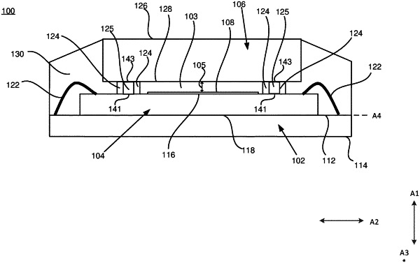
1. A method for fabricating an image sensor package to define a gap height, the method comprising:
coupling an image sensor die to a substrate;
forming a plurality of pillar members on the image sensor die;
dispensing a bonding material on the plurality of pillar members;
contacting a transparent member with the bonding material such that a height of the plurality of pillar members defines a gap height between an active region of the image sensor die and the transparent member, the bonding material contacting a side of a pillar member, from the plurality of pillar members, that extends between a first end contacting the transparent member and a second end contacting the image sensor die; and
curing the bonding material to couple the transparent member to the image sensor die.
|