| CPC H01L 27/14618 (2013.01) [H01L 27/14625 (2013.01); H01L 27/14636 (2013.01)] | 17 Claims |
|
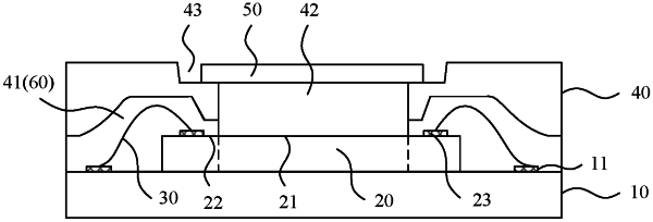
1. A photosensitive chip package structure, comprising a substrate and a photosensitive chip mounted on the substrate, wherein a side of the photosensitive chip away from the substrate has a photosensitive area and a non-photosensitive area surrounding the photosensitive area, and the photosensitive chip is electrically connected to the substrate using a metal wire; and further comprising:
a frame, disposed on the side of the photosensitive chip away from the substrate, wherein an avoidance groove used to avoid the metal wire is disposed on a side of the frame facing the substrate, wherein the avoidance groove extends along a side edge of the frame, and an inner wall of the avoidance groove is an arc-shaped inner wall; and
a filling glue, filled in the avoidance groove, wrapping around the metal wire and bonding the frame to the non-photosensitive area of the photosensitive chip and the substrate.
|