| CPC H01L 27/1288 (2013.01) [H01L 24/03 (2013.01); H01L 24/05 (2013.01); H01L 25/167 (2013.01); H01L 27/1248 (2013.01); H01L 24/08 (2013.01); H01L 2224/03614 (2013.01); H01L 2224/03622 (2013.01); H01L 2224/05567 (2013.01); H01L 2224/08145 (2013.01); H01L 2924/12041 (2013.01)] | 19 Claims |
|
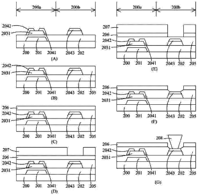
1. A method for fabricating an array substrate, comprising:
providing a substrate;
forming an array layer on the substrate; wherein the array layer comprises a thin film transistor and a conductive pad spaced apart in a direction parallel to the substrate;
forming a passivation layer on the array layer, wherein the passivation layer covers the thin film transistor and the conductive pad;
forming a full-surface carbon film on the passivation layer; and
removing the passivation layer and the carbon film corresponding to the conductive pad by a patterning process to obtain the array substrate;
wherein the step of removing the passivation layer and the carbon film corresponding to the conductive pad by the patterning process comprises:
forming a photoresist layer on a surface of the carbon film away from the passivation layer;
patterning the photoresist layer to obtain a patterned photoresist layer with an opening corresponding to the conductive pad;
sequentially removing part of the carbon film and part of the passivation layer corresponding to the opening to expose the conductive pad; wherein the carbon film forms a patterned carbon film covering the thin film transistor, and the patterned carbon film is a light-shielding layer.
|