| CPC H01L 27/124 (2013.01) [H01L 23/60 (2013.01); H01L 25/18 (2013.01)] | 11 Claims |
|
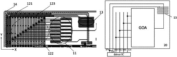
1. A Gate on Array (GOA) circuit comprising:
a GOA area, wherein the GOA area comprises a plurality of GOA unit circuits cascaded with each other; and
a lead area, wherein at least one Start Vertical (STV) signal line and at least one Non-Start Vertical (non-STV) signal line are arranged in the lead area, each STV signal line and each non-STV signal line is connected to at least one GOA unit circuit, and the non-STV signal line comprises at least one of a Vdd signal line, a clock (Clk) signal line, a Gate High Voltage (VGH) signal line and a Gate Low Voltage (VGL) signal line; a projection of the at least one STV signal line on the lead area does not overlap a projection of the at least one non-STV signal line on the lead area;
wherein the GOA circuit further comprises an electro-static discharge electrode disposed at a different layer from the STV signal line, a projection of the electro-static discharge electrode on the lead area overlaps a projection of the STV signal line on the lead area, and a gate insulation layer is provided between the electro-static discharge electrode and the STV signal line.
|