| CPC H01L 27/124 (2013.01) [H01L 27/127 (2013.01); H01L 27/1251 (2013.01)] | 20 Claims |
|
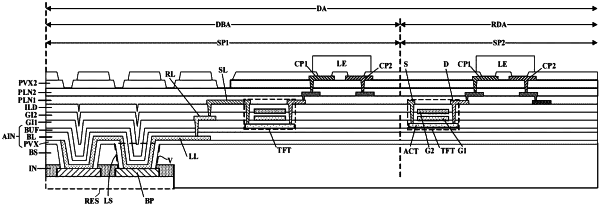
1. An array substrate, comprising a display area having a plurality of subpixels;
wherein the display area comprises a regular display sub-area and a display-bonding sub-area;
the plurality of subpixels comprises a plurality of first subpixels in the display-bonding sub-area and a plurality of second subpixels in the regular display sub-area;
wherein the array substrate comprises:
a base substrate extending throughout the regular display sub-area and the display-bonding sub-area; and
a plurality of thin film transistors on a first side of the base substrate and respectively in the plurality of subpixels;
wherein a respective one of the plurality of first subpixels comprises:
a bonding pad on a second side of the base substrate, wherein the second side is opposite to the first side;
a lead line electrically connecting a respective one of the plurality of thin film transistors to the bonding pad, wherein the lead line is unexposed in the array substrate; and
a via extending through the base substrate;
wherein the lead line extends from the first side to the second side of the base substrate through the via, to connect to the bonding pad.
|