US 11,869,896 B2
Display device having a semiconductor layer with a mesh structure
Woo Bin Lee, Hwaseong-si (KR); Seok Hwan Bang, Yongin-si (KR); Seung Sok Son, Goyang-si (KR); Woo Geun Lee, Suwon-si (KR); and Soo Jung Chae, Seoul (KR)
Assigned to Samsung Display Co., Ltd., Yongin-si (KR)
Filed by Samsung Display Co., Ltd., Yongin-Si (KR)
Filed on Jul. 6, 2021, as Appl. No. 17/368,200.
Claims priority of application No. 10-2020-0143366 (KR), filed on Oct. 30, 2020.
Prior Publication US 2022/0139965 A1, May 5, 2022
Int. Cl. H01L 27/12 (2006.01); H10K 59/121 (2023.01); H10K 77/10 (2023.01); H10K 102/00 (2023.01)
CPC H01L 27/1222 (2013.01) [H01L 27/1218 (2013.01); H01L 27/1225 (2013.01); H10K 59/1213 (2023.02); H10K 77/111 (2023.02); H10K 2102/311 (2023.02)] 19 Claims
OG exemplary drawing
 
1. A display device comprising:
a substrate; and
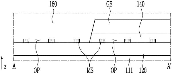
a transistor disposed on the substrate and including a semiconductor layer and a gate electrode,
wherein the semiconductor layer includes a mesh structure, and
wherein a plurality of openings are formed in the semiconductor layer, and at least some of the plurality of the openings overlap the gate electrode.