| CPC H01L 27/0924 (2013.01) [H01L 21/02532 (2013.01); H01L 21/31116 (2013.01); H01L 21/76224 (2013.01); H01L 21/823807 (2013.01); H01L 21/823814 (2013.01); H01L 21/823828 (2013.01); H01L 21/823878 (2013.01); H01L 29/0673 (2013.01); H01L 29/0847 (2013.01); H01L 29/1037 (2013.01); H01L 29/165 (2013.01); H01L 29/41758 (2013.01); H01L 29/6653 (2013.01); H01L 29/6656 (2013.01); H01L 29/66545 (2013.01)] | 8 Claims |
|
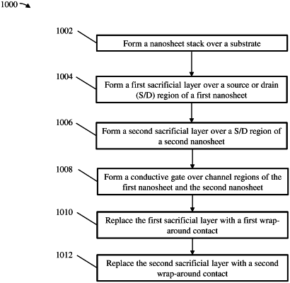
1. A semiconductor device comprising:
a nanosheet stack over a substrate, the nanosheet stack comprising a top portion and a bottom portion separated by a dielectric spacer;
a plurality of vertically stacked first source or drain (S/D) regions, each of the first S/D regions on a sidewall of a different nanosheet in the bottom portion of the nanosheet stack, each of the first S/D regions confined to the respective sidewall of one nanosheet such that none of the plurality of first S/D regions merge and each sidewall of the different nanosheets in the bottom portion is covered by a separate first S/D region;
a plurality of vertically stacked second S/D regions, each of the second S/D regions on a sidewall of a different nanosheet in the top portion of the nanosheet stack, each of the second S/D regions confined to the respective sidewall of one nanosheet such that none of the plurality of second S/D regions merge and each sidewall of the different nanosheets in the top portion is covered by a separate second S/D region;
a first wrap-around contact formed over the first plurality of S/D regions; and
a second wrap-around contact formed over the second plurality of S/D regions.
|