| CPC H01L 27/0629 (2013.01) [H01L 21/823418 (2013.01); H01L 21/823437 (2013.01)] | 20 Claims |
|
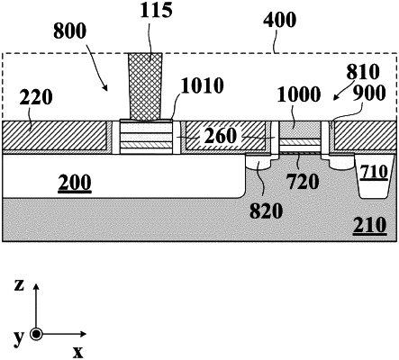
1. A semiconductor structure, comprising:
a semiconductor substrate with spaced apart first and second isolation regions formed therein, wherein the first isolation region is wider than the second isolation region;
a resistor structure disposed on the first isolation region, wherein the resistor structure comprises:
a dielectric layer in contact with the first isolation region;
a nitride layer disposed on the dielectric layer;
a semiconductor layer disposed on the nitride layer, the semiconductor layer comprising a top doped layer overlying a bottom un-doped layer; and
a silicide covering an entire surface of the top doped layer; and
a transistor structure disposed between the first and second isolation regions, wherein the transistor structure comprises:
an interfacial layer in contact with the substrate, wherein the dielectric layer is disposed on the interfacial layer;
a metal gate electrode disposed on the dielectric layer; and
a source/drain region formed in the substrate and adjacent to the metal gate electrode.
|