| CPC H01L 25/0657 (2013.01) [H01L 21/76898 (2013.01); H01L 23/32 (2013.01); H01L 23/481 (2013.01); H01L 24/19 (2013.01); H01L 24/20 (2013.01); H01L 24/73 (2013.01); H01L 24/83 (2013.01); H01L 25/50 (2013.01); H01L 2224/2101 (2013.01); H01L 2224/32146 (2013.01); H01L 2224/73267 (2013.01); H01L 2224/83896 (2013.01); H01L 2225/06541 (2013.01); H01L 2924/37001 (2013.01)] | 19 Claims |
|
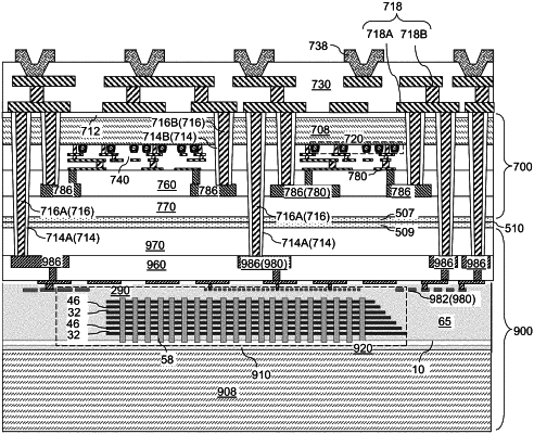
1. A bonded assembly, comprising:
a first semiconductor die comprising a first substrate, first semiconductor devices located on the first substrate, first dielectric material layers located on the first semiconductor devices, and first metal interconnect structures embedded in the first dielectric material layers;
a second semiconductor die overlying the first semiconductor die, and comprising a second substrate, second semiconductor devices located on the second substrate, second dielectric material layers located on the second semiconductor devices, and second metal interconnect structures embedded in the second dielectric material layers;
first conductive via structures vertically extending through the second substrate, the second dielectric material layers, and a respective subset of the first dielectric material layers, and contacting a respective one of the first metal interconnect structures;
second conductive via structures vertically extending through the second substrate and a respective subset of the second dielectric material layers, and contacting a respective one of the second metal interconnect structures; and
redistribution metal interconnect structures located over a backside surface of the second substrate and electrically connecting the first conductive via structures to the second conductive via structures;
wherein:
the first semiconductor die further comprises a first bonding dielectric material layer;
the second semiconductor die further comprises a second bonding dielectric material layer;
the second semiconductor die is bonded to the first semiconductor die via dielectric-to-dielectric bonding at a horizontal bonding interface at which the second bonding dielectric material layer is in direct contact with the first bonding dielectric layer, the horizontal bonding interface including discrete openings therethrough;
first conductive via structures each have a respective vertically-extending sidewall that vertically extends through the second substrate, the second dielectric material layers, the second bonding dielectric material layer, a respective one of the discrete openings through the horizontal bonding interface, the first bonding dielectric material layer, and the respective subset of the first dielectric material layers;
each of the first bonding dielectric material layer and the second bonding dielectric material layer does not laterally surround any conductive structure other than the first conductive via structures; and
there are no metal bonding pads in a horizontal plane of the horizontal bonding interface.
|