US 11,869,876 B2
Thinning system in package
Chun Jung Lin, Kaohsiung (TW); and Ruei Ting Gu, Kaohsiung (TW)
Assigned to WALTON ADVANCED ENGINEERING INC., Kaohsiung (TW)
Filed by WALTON ADVANCED ENGINEERING INC., Kaohsiung (TW)
Filed on Jun. 22, 2021, as Appl. No. 17/353,861.
Claims priority of application No. 110108822 (TW), filed on Mar. 12, 2021.
Prior Publication US 2022/0293562 A1, Sep. 15, 2022
Int. Cl. H01L 23/49 (2006.01); H01L 25/065 (2023.01); H01L 23/00 (2006.01)
CPC H01L 25/0657 (2013.01) [H01L 23/49 (2013.01); H01L 24/32 (2013.01); H01L 24/48 (2013.01); H01L 24/73 (2013.01); H01L 2224/32245 (2013.01); H01L 2224/48145 (2013.01); H01L 2224/48195 (2013.01); H01L 2224/48245 (2013.01); H01L 2224/73265 (2013.01); H01L 2225/0651 (2013.01); H01L 2225/06506 (2013.01); H01L 2225/06582 (2013.01)] 10 Claims
OG exemplary drawing
 
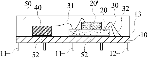
1. A thinning system in package featuring an encapsulation structure in which no printed circuit board exist and comprising: a copper holder with a plurality of data pins and at least a ground pin; a plurality of dies mounted on the top face of the copper holder and electrically connected to the data pins of the copper holder; at least a passive element mounted on the top face of the copper holder and electrically connected to the dies wherein both the dies and the passive element are fixed on the top face of the copper holder through a layer of insulation adhesives and the dies are electrically connected to the ground pin of the copper holder; a molding compound encasing the dies and the passive element on the top face of the copper holder.