| CPC H01L 25/0652 (2013.01) [H01L 21/76802 (2013.01); H01L 21/76843 (2013.01); H01L 21/76877 (2013.01); H01L 23/49827 (2013.01); H01L 24/08 (2013.01); H01L 24/80 (2013.01); H01L 25/50 (2013.01); H01L 2224/08113 (2013.01); H01L 2224/08146 (2013.01); H01L 2224/80896 (2013.01); H01L 2924/15153 (2013.01)] | 19 Claims |
|
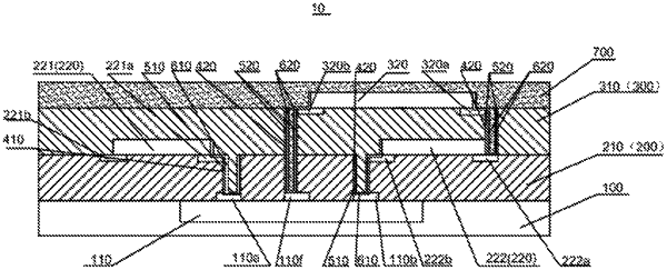
1. A chip stack packaging structure, comprising:
a base chip layer, comprising a base chip having pins on a front surface;
at least one stacked chip layer, which is sequentially formed on the base chip layer, has an inter-chip insulating layer and at least one stacked chip attached to the inter-chip insulating layer and having a plurality of pins on a front surface, wherein the front surface of the at least one stacked chip faces the front surface of the base chip; and
a top insulating layer, stacked on a stacked chip layer farthest from the base chip layer,
wherein a vertical interconnection hole is formed inside the inter-chip insulating layer to allow corresponding pins to be communicated vertically, wherein the corresponding pins refer to specified pins that need to be electrically connected,
inside the vertical interconnection hole, a conductive material layer is formed, which makes the corresponding pins electrically connected,
and the at least one stacked chip is thinned and reduced after attached to the inter-chip insulating layer, so as to expose a part of area of pins of the at least one stacked chip, so as to realize a vertical connection of the at least one stacked chip with other chips through the pins;
wherein the pins of the base chip are embedded in the inter-chip insulating layer of the at least one stacked chip layer adjacent to the base chip layer, and the pins of the at least one stacked chip are embedded in an inter-chip insulating layer of a stacked chip layer where the at least one stacked chip is located.
|