| CPC H01L 24/80 (2013.01) [H01L 24/08 (2013.01); H01L 2224/08145 (2013.01); H01L 2224/80895 (2013.01); H01L 2224/80896 (2013.01)] | 20 Claims |
|
1. A method comprising:
putting a first package component into contact with a second package component, wherein:
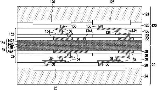
the first package component comprises a first dielectric layer comprising a first dielectric material, wherein the first dielectric material is a silicon-oxide-based dielectric material;
the second package component comprises a second dielectric layer comprising a second dielectric material different from the first dielectric material, wherein the second dielectric material comprises silicon and an element selected from the group consisting of carbon, nitrogen, and combinations thereof, and wherein before the first package component is put to contact with the second package component, no treatment process using nitrogen (N2) is preformed, and no treatment process using oxygen (O2) is performed; and
performing an annealing process to bond the first dielectric layer to the second dielectric layer.
|