| CPC H01L 24/37 (2013.01) [H01L 24/84 (2013.01); H01L 2224/37012 (2013.01); H01L 2224/84345 (2013.01); H01L 2224/84815 (2013.01); H01L 2924/3656 (2013.01)] | 7 Claims |
|
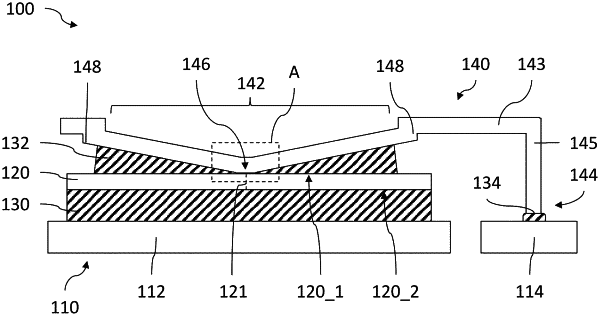
1. A semiconductor device, comprising:
a carrier comprising a die pad and a contact;
a semiconductor die comprising a first main side and an opposing second main side, the semiconductor die being attached to the die pad by a first solder joint such that the second main side faces the die pad; and
a contact clip comprising a first contact region and a second contact region, the first contact region being attached to the first main side of the semiconductor die by a second solder joint and the second contact region being attached to the contact by a third solder joint,
wherein the first contact region has a convex shape facing towards the first main side of the semiconductor die such that a distance between the first main side and the first contact region increases from a base of the convex region towards an edge of the first contact region,
wherein the base runs along a line that runs substantially perpendicular to a longitudinal axis of the contact clip.
|