| CPC H01L 24/06 (2013.01) [H01L 24/08 (2013.01); H01L 24/32 (2013.01); H01L 24/83 (2013.01); H01L 23/585 (2013.01); H01L 24/05 (2013.01); H01L 24/29 (2013.01); H01L 2224/05647 (2013.01); H01L 2224/06517 (2013.01); H01L 2224/08145 (2013.01); H01L 2224/2919 (2013.01); H01L 2224/29186 (2013.01); H01L 2224/32145 (2013.01); H01L 2224/80203 (2013.01); H01L 2224/80895 (2013.01); H01L 2224/8385 (2013.01); H01L 2224/83203 (2013.01); H01L 2224/83896 (2013.01)] | 20 Claims |
|
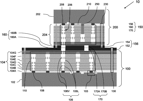
1. A die stack comprising:
a first die comprising a first semiconductor substrate;
a second die comprising a second semiconductor substrate;
a bonding dielectric structure (BDS) comprising a bonding polymer, wherein the BDS bonds the first die and the second die;
a bonding interconnect structure (BIS) that extends through the BDS to bond and electrically connect the first die and the second die; and
a bonding dummy pattern (BDP) that extends through the BDS to bond the first die and the second die, wherein the BDP is electrically conductive and is electrically floated,
wherein a pattern density of the BDP in the BDS is from 80% to 40%.
|