| CPC H01L 23/552 (2013.01) [H01L 21/4853 (2013.01); H01L 21/4871 (2013.01); H01L 21/565 (2013.01); H01L 21/78 (2013.01); H01L 23/3121 (2013.01); H01L 23/3675 (2013.01); H01L 23/49838 (2013.01)] | 2 Claims |
|
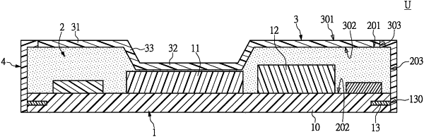
1. A package structure, comprising:
a circuit board including a substrate and a first electronic element disposed on the substrate;
a mold sealing layer disposed on the substrate and covering the first electronic element, the mold sealing layer having a top surface, a bottom surface corresponding to the top surface, and a side surface connected between the top surface and the bottom surface;
a conductive metal board disposed on the top surface and adjacent to the first electronic element; and
a conductive layer disposed on the side surface;
wherein the conductive metal board and the conductive layer are each an independent component;
wherein the conductive metal board has a top face, a bottom face corresponding to the top face, and a side face connected between the top face and the bottom face;
wherein the circuit board further includes a conductive ground element embedded into the substrate;
wherein the conductive ground element has an exposed surface for which the substrate is exposed, the conductive layer is bent and directly contacts the side surface, the side face, the top surface, and the exposed surface, and the conductive layer is electrically connected to the conductive metal board and the conductive ground element.
|