| CPC H01L 23/5386 (2013.01) [H01L 24/16 (2013.01); H01L 25/18 (2013.01); H10B 80/00 (2023.02); H01L 25/0657 (2013.01); H01L 2224/16225 (2013.01); H01L 2225/06517 (2013.01); H01L 2225/06565 (2013.01)] | 20 Claims |
|
1. An interposer routing structure, comprising:
a first trace layer comprising a first ground trace and a first power trace, wherein the first trace layer is configured to receive power;
a bump layer coupled to a die;
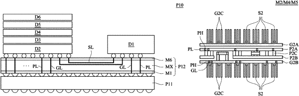
a second trace layer coupled to the first ground trace and the first power trace, and comprising a plurality of second ground traces, a plurality of second power traces and at least one connecting power trace, wherein the plurality of second ground traces are located on both sides of the plurality of second power traces, so that the plurality of second ground traces isolate the plurality of second power traces from a plurality of signal traces in the second trace layer, and the plurality of second power traces are coupled to each other by the at least one connecting power trace; and
a third trace layer coupled to the first ground trace and the first power trace, and comprising a plurality of third ground traces, at least one third power trace, a plurality of connecting ground traces and a plurality of branch ground traces, wherein the plurality of third ground traces are located on both sides of the at least one third power trace, so that the plurality of third ground traces isolate the at least one third power trace from a plurality of signal traces in the third trace layer; and
wherein the plurality of third ground traces are coupled to each other by the plurality of connecting ground traces, and the plurality of branch ground traces are located on both sides of the plurality of signal traces in the third trace layer.
|
|
11. A semiconductor package, comprising:
at least one die;
a substrate configured to receive power, and coupled to a ground potential; and
an interposer layer coupled between the substrate and the at least one die, and comprising:
a first trace layer comprising a first ground trace and a first power trace, so as to coupled to the substrate;
a second trace layer coupled to the first trace layer, and comprising a plurality of second ground traces, a plurality of second power traces and at least one connecting power trace,
wherein the plurality of second ground traces are located on both sides of the plurality of second power traces, so that the plurality of second ground traces isolate the plurality of second power traces from a plurality of signal traces in the second trace layer, and the plurality of second power traces are coupled to each other by the at least one connecting power trace; and
a third trace layer coupled to the first trace layer, and comprising a plurality of third ground traces, at least one third power trace, a plurality of connecting ground traces and a plurality of branch ground traces, wherein the plurality of third ground traces are located on both sides of the at least one third power trace, so that the plurality of third ground traces isolate the at least one third power trace from a plurality of signal traces in the third trace layer; and
wherein the plurality of third ground traces are coupled to each other by the plurality of connecting ground traces, and the plurality of branch ground traces are located on both sides of the plurality of signal traces in the third trace layer.
|