| CPC H01L 23/5384 (2013.01) [G11C 11/221 (2013.01); H10B 53/20 (2023.02)] | 20 Claims |
|
1. A method of fabricating a device structure, the method comprising:
forming a first conductive interconnect in a first dielectric in a memory region and a second conductive interconnect in the first dielectric in a logic region;
depositing an etch stop layer on the first dielectric and on the first conductive interconnect and on the second conductive interconnect;
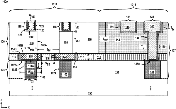
forming a first electrode structure on the first conductive interconnect by a first process comprising:
etching a first opening in the etch stop layer;
depositing a first conductive hydrogen barrier layer in the first opening; and
depositing a conductive material on the first conductive hydrogen barrier layer;
forming a memory device by depositing a material layer stack comprising a ferroelectric material or a paraelectric material on the first electrode structure and etching the material layer stack;
depositing a second dielectric comprising an amorphous greater than 90% film density hydrogen barrier material on the memory device and on the etch stop layer;
etching and removing the second dielectric from the logic region and depositing a third dielectric comprising a first less than 90% film density material;
etching the third dielectric to form a first via opening and exposing the second conductive interconnect;
filling the first via opening with a first one or more conductive materials to form a via structure;
depositing a fourth dielectric comprising a second less than 90% film density material on the third dielectric and on the via structure;
forming a trench opening in the fourth dielectric and exposing the via structure;
depositing a second one or more conductive materials in the trench opening on the via structure to form a metal line; and
forming a via electrode on the memory device by a second process comprising:
forming a hanging trench in the fourth dielectric and exposing the third dielectric;
forming a mask on a portion of the hanging trench, the mask providing a second opening that exposes a portion of the second dielectric;
etching the second dielectric through the second opening to form a second via opening, the second via opening exposing the memory device;
depositing a second conductive hydrogen barrier layer on a first uppermost surface of the memory device, in the second via opening, and in the hanging trench;
depositing a third one or more conductive materials on the second conductive hydrogen barrier layer in the second via opening; and planarizing to form a contact electrode in the hanging trench, and the via electrode.
|