| CPC H01L 23/5381 (2013.01) [H01L 23/49816 (2013.01); H01L 23/49822 (2013.01); H01L 23/49838 (2013.01); H01L 23/5383 (2013.01); H01L 23/5384 (2013.01); H01L 23/5386 (2013.01)] | 17 Claims |
|
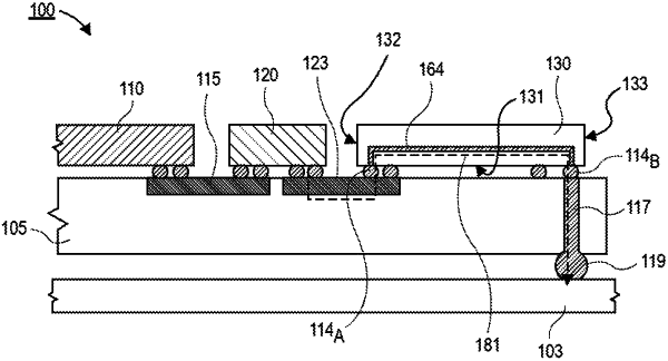
1. An electronic package, comprising:
a package substrate, wherein the package substrate comprises a first routing architecture;
a first die on the package substrate;
a second die on the package substrate, wherein the first die is electrically coupled to the second die by a bridge embedded in the package substrate; and
a routing patch on the package substrate, wherein the routing patch is a discrete component coupled to a same side of the package substrate as the second die and is laterally spaced apart from the second die, wherein the routing patch is electrically coupled to the second die by a trace in the package substrate, and wherein the routing patch comprises a second routing architecture that is different than the first routing architecture.
|