| CPC H01L 23/535 (2013.01) [H01L 21/76805 (2013.01); H01L 21/76895 (2013.01); H01L 23/5283 (2013.01); H10B 41/27 (2023.02); H10B 41/41 (2023.02); H10B 43/27 (2023.02); H10B 43/40 (2023.02)] | 7 Claims |
|
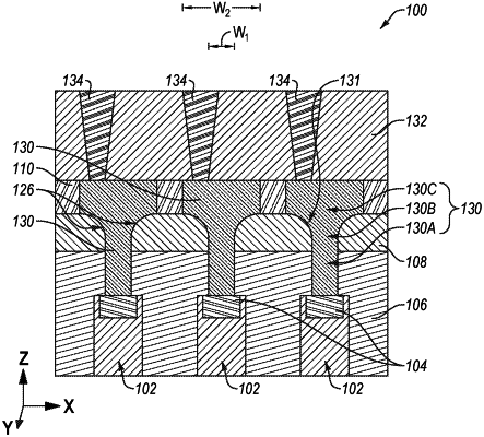
1. A microelectronic device, comprising:
pillar structures comprising semiconductive material;
contact structures in physical contact with upper portions of the pillar structures;
conductive structures over and in physical contact with the contact structures, each of the conductive structures being substantially monolithic and comprising:
a lower portion having first substantially linear boundaries in a vertically oriented plane and a first maximum horizontal width;
an upper portion vertically overlying the lower portion, the upper portion having second substantially linear boundaries in the vertically oriented plane and a second maximum horizontal width greater than the first maximum horizontal width; and
an additional portion vertically interposed between the lower portion and the upper portion and having arcuate boundaries in the vertically oriented plane, the arcuate boundaries exhibiting a radiused, concave shape in the vertically oriented plane and defining additional horizontal widths progressively increasing from the first maximum horizontal width proximate the lower portion to a relatively larger horizontal width proximate the upper portion;
a first dielectric oxide material substantially horizontally surrounding the lower portion of each of the conductive structures along an entire vertical height of the lower portion;
a second dielectric material overlying the first dielectric oxide material and substantially horizontally surrounding the additional portion of each of the conductive structures along an entire vertical height of the additional portion, the second dielectric material having arcuate edges exhibiting a radiused, convex shape in the vertically oriented plane and opposing the arcuate boundaries of the additional portion of each of the conductive structures; and
a third dielectric oxide material overlying the second dielectric material and substantially horizontally surrounding the upper portion of each of the conductive structures along an entire vertical height of the upper portion.
|