| CPC H01L 23/49838 (2013.01) [G06F 3/044 (2013.01); H01L 21/4857 (2013.01); H01L 23/49866 (2013.01); H01L 33/62 (2013.01); H05K 1/09 (2013.01); H05K 3/4007 (2013.01); H01L 2933/0066 (2013.01); H05K 2201/0338 (2013.01); H05K 2201/0341 (2013.01); H05K 2203/04 (2013.01)] | 12 Claims |
|
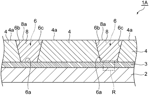
1. An electroconductive substrate comprising:
a base material;
a trench formation layer on one side of the base material; and
an electroconductive pattern layer, wherein:
the trench formation layer includes a trench with (i) a bottom surface facing the base material and (ii) a first inclined lateral surface that is inclined from the bottom surface outwardly;
the trench is at least partially filled with the electroconductive pattern layer;
the electroconductive pattern layer in the trench has a second inclined lateral surface facing the first inclined lateral surface and inclined in a same direction as the first inclined lateral surface; and
there is a gap between the first inclined lateral surface and the second inclined lateral surface.
|