| CPC H01L 23/49822 (2013.01) [H01L 21/4857 (2013.01); H01L 23/49838 (2013.01); H01L 23/3128 (2013.01); H01L 24/16 (2013.01); H01L 2224/16227 (2013.01)] | 14 Claims |
|
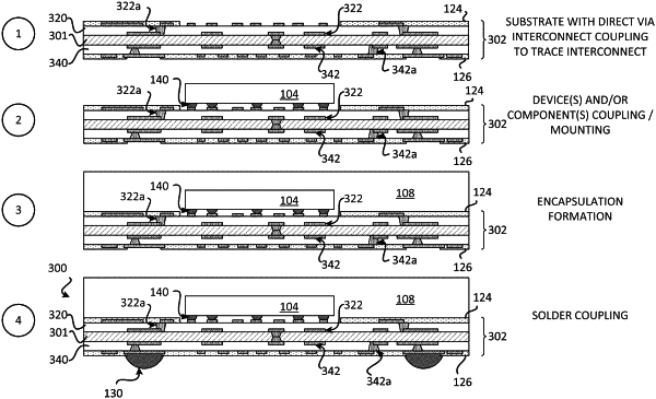
1. A package comprising:
a substrate comprising:
a plurality of interconnects comprising:
a first via interconnect that includes a first width and
a first trace interconnect directly coupled to a side portion of the first via interconnect;
a second trace interconnect directly coupled to a first surface of the first via interconnect;
wherein the first trace interconnect includes a second width that is less than the first width and the second trace interconnect includes a third width that is less than the first width;
at least one dielectric layer at least partially surrounding the plurality of interconnects; and
an integrated device coupled to the substrate and located over the substrate, wherein the at least one dielectric layer and the plurality of interconnects are located in planes underneath the integrated device.
|