| CPC H01L 23/49541 (2013.01) [H01L 23/3107 (2013.01); H01L 23/49503 (2013.01); H01L 24/48 (2013.01); H01L 2224/48175 (2013.01)] | 16 Claims |
|
1. A semiconductor package, comprising:
a die attach pad;
a plurality of lead terminals positioned about the die attach pad and disposed along side edges of the semiconductor package;
a semiconductor die mounted on the die attach pad;
a molding compound encapsulating the plurality of lead terminals and the semiconductor die; and
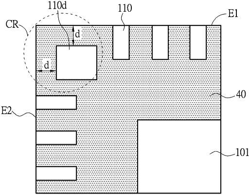
at least one dummy lead disposed in a corner region of the semiconductor package between the plurality of lead terminals, wherein the at least one dummy lead disposed in the corner region is kept a predetermined distance away from adjacent two side edges of the semiconductor package, and therefore does not have an exposed end surface on any of the adjacent two side edges.
|