| CPC H01L 23/482 (2013.01) [H01L 23/3128 (2013.01); H01L 23/481 (2013.01); H01L 23/49816 (2013.01); H01L 23/49827 (2013.01); H01L 24/73 (2013.01); H01L 25/03 (2013.01); H01L 25/0657 (2013.01); H01L 25/10 (2013.01); H01L 23/5389 (2013.01); H01L 24/16 (2013.01); H01L 24/24 (2013.01); H01L 24/32 (2013.01); H01L 2224/04105 (2013.01); H01L 2224/06181 (2013.01); H01L 2224/13025 (2013.01); H01L 2224/16227 (2013.01); H01L 2224/16237 (2013.01); H01L 2224/16238 (2013.01); H01L 2224/17181 (2013.01); H01L 2224/244 (2013.01); H01L 2224/24227 (2013.01); H01L 2224/32145 (2013.01); H01L 2224/32225 (2013.01); H01L 2224/73253 (2013.01); H01L 2224/73259 (2013.01); H01L 2224/73265 (2013.01); H01L 2224/73267 (2013.01); H01L 2224/81191 (2013.01); H01L 2224/92224 (2013.01); H01L 2225/0651 (2013.01); H01L 2225/06517 (2013.01); H01L 2225/06548 (2013.01); H01L 2225/06572 (2013.01); H01L 2225/06582 (2013.01); H01L 2924/15311 (2013.01); H01L 2924/15331 (2013.01); H01L 2924/181 (2013.01); H01L 2924/18161 (2013.01); H01L 2924/19107 (2013.01)] | 12 Claims |

|
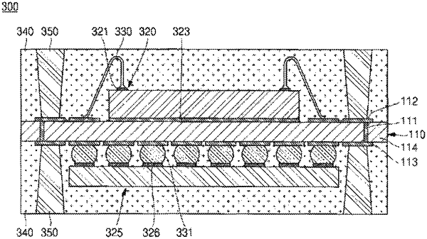
1. A semiconductor device, comprising:
a substrate having a top major surface and a bottom major surface opposite to the top major surface;
an electrically conductive pattern adjoining the top major surface;
conductive lands adjoining the bottom major surface and including a first conductive land, a second conductive land, a third conductive land, and a fourth conductive land;
conductive vias within the substrate and connecting part of the electrically conductive pattern to the conductive lands, the conductive vias including a first conductive via having a first width in a cross-sectional view and connected to the third conductive land;
conductive bumps;
a first semiconductor die mounted to the first conductive land and the second conductive land with the conductive bumps;
an electronic component electrically connected to the electrically conductive pattern of the substrate and mounted on the top major surface of the substrate;
a first package body encapsulating the first semiconductor die and comprising a bottom exterior surface distal to the bottom major surface of the substrate;
a second package body encapsulating the electronic component;
a first electrically conductive path physically and electrically connected to the third conductive land and extending to the bottom exterior surface of the first package body having a second width in the cross-sectional view that is greater than the first width; and
a second electrically conductive path physically and electrically connected to the fourth conductive land and extending to the bottom exterior surface of the first package body, wherein:
the first electrically conductive path comprises a first outer surface exposed from the bottom exterior surface of the first package body and configured as a first external electrical interconnect structure; and
the second electrically conductive path comprises a second outer surface exposed from the bottom exterior surface of the first package body and configured as a second external electrical interconnect structure.
|