| CPC H01L 23/481 (2013.01) [H01L 21/76898 (2013.01); H01L 27/01 (2013.01); H01L 24/05 (2013.01); H01L 2224/05541 (2013.01); H01L 2224/05647 (2013.01); H01L 2224/05684 (2013.01)] | 10 Claims |
|
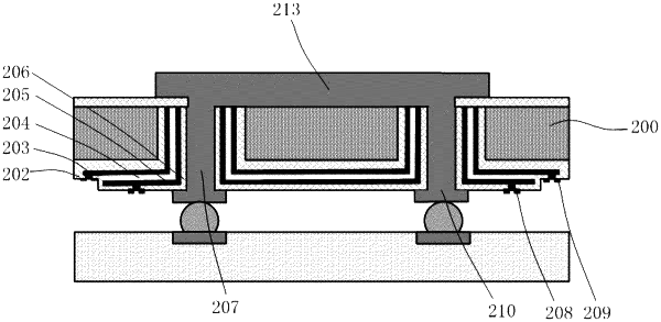
1. A three-dimensional capacitor-inductor based on a high-functional-density through silicon via structure, comprising:
a substrate formed with a through silicon via;
a three-dimensional capacitor, formed on a sidewall of the through silicon via, and sequentially including a first metal layer, a second insulating layer, and a second metal layer; and
a three-dimensional inductor, composed center-filled metal of the through silicon via and planar thick metal rewiring,
wherein a first insulating layer is provided between the sidewall of the through silicon via and the three-dimensional capacitor, and a third insulating layer is provided between the three-dimensional capacitor and the three-dimensional inductor.
|