| CPC H01L 23/42 (2013.01) [H01L 21/561 (2013.01); H01L 21/568 (2013.01); H01L 21/762 (2013.01); H01L 23/3135 (2013.01); H01L 23/5226 (2013.01); H01L 23/66 (2013.01); H01L 24/11 (2013.01); H01L 24/13 (2013.01); H01L 24/14 (2013.01); H01L 24/73 (2013.01); H01L 2224/1319 (2013.01); H01L 2224/13024 (2013.01); H01L 2224/13147 (2013.01); H01L 2224/141 (2013.01); H01L 2224/73104 (2013.01); H01L 2924/014 (2013.01)] | 18 Claims |
|
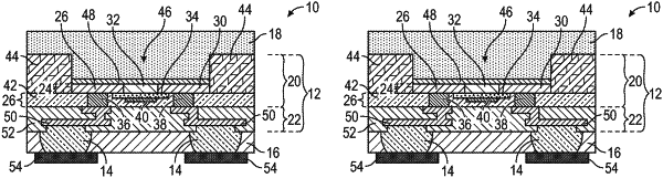
1. A method comprising:
forming a device wafer with a plurality of device dies, each of which includes an active layer;
applying a first mold compound over a bottom surface of the device wafer to encapsulate a plurality of first bump structures of each of the plurality of device dies of the device wafer;
removing a silicon handle substrate completely from the device wafer to provide an etched wafer, wherein:
the silicon handle substrate is directly over each of a plurality of interfacial layers, which is directly over the active layer of a corresponding one of the plurality of device dies, respectively; and
each of the plurality of interfacial layers is formed of silicon germanium (SiGe);
applying a second mold compound over the active layer of each of the plurality of device dies from where the silicon handle substrate is removed, wherein no silicon material resides between the second mold compound and each active layer; and
thinning the first mold compound until exposing a bottom portion of each of the plurality of first bump structures.
|