| CPC H01L 23/3157 (2013.01) [H01L 24/16 (2013.01); H01L 24/32 (2013.01); H01L 24/73 (2013.01); H01L 25/0655 (2013.01); H01L 25/50 (2013.01); H01L 2224/16227 (2013.01); H01L 2224/32225 (2013.01); H01L 2224/73204 (2013.01)] | 20 Claims |
|
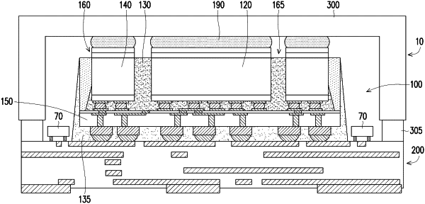
1. A semiconductor package, comprising:
a redistribution structure;
a plurality of semiconductor devices mounted on the redistribution structure; and
a plurality of heat dissipation films respectively disposed on and jointly covering upper surfaces of the plurality of semiconductor devices, wherein a plurality of trenches are respectively extended between each two of the plurality of heat dissipation films; and
an encapsulating material disposed on the redistribution structure and encapsulating the plurality of semiconductor devices, wherein a first surface of the encapsulating material faces the redistribution structure, and a second surface opposite to the first surface of the encapsulating material is exposed from the plurality of trenches.
|