| CPC H01L 23/3128 (2013.01) [H01L 21/561 (2013.01); H01L 23/481 (2013.01); H01L 25/0652 (2013.01); H01L 25/0657 (2013.01); H01L 25/50 (2013.01); H01L 2225/06541 (2013.01)] | 20 Claims |
|
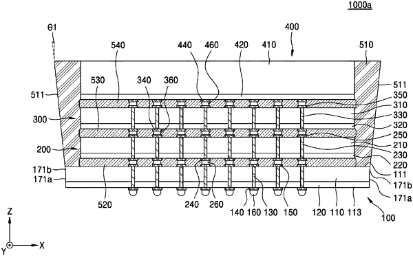
1. A semiconductor package comprising:
a first semiconductor chip comprising a first surface and a second surface opposite to each other;
at least one second semiconductor chip stacked on the first surface of the first semiconductor chip; and
a molding layer contacting the first surface of the first semiconductor chip and a side wall of the at least one second semiconductor chip,
wherein an external side wall of the molding layer comprises:
a first external side wall portion extending from a lower end of the molding layer adjacent to the first semiconductor chip, to a first height to be inclined outward with respect to a vertical direction perpendicular to the first surface of the first semiconductor chip; and
a second external side wall portion extending from the first height to a second height to be inclined inward with respect to the vertical direction,
wherein the first external side wall portion of the molding layer extends, as a first slope, from the lower end of the molding layer to the first height, and
wherein the side wall of the at least one second semiconductor chip is not parallel to the first external side wall portion of the molding layer and the second external side wall portion of the molding layer.
|