| CPC H01L 22/32 (2013.01) [H01L 23/3157 (2013.01); H01L 23/49822 (2013.01); H01L 24/05 (2013.01); H01L 24/06 (2013.01); H01L 24/13 (2013.01); H01L 2224/0217 (2013.01); H01L 2224/0401 (2013.01); H01L 2224/05556 (2013.01); H01L 2224/06515 (2013.01); H01L 2224/13007 (2013.01)] | 20 Claims |
|
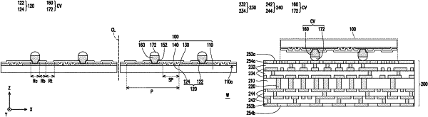
1. An integrated circuit component, comprising:
a semiconductor substrate;
conductive pads, disposed on and electrically coupled to the semiconductor substrate, and each having a contact region and a testing region next to the contact region, wherein a surface roughness of a surface of the testing region of the at least one of the conductive pads is greater than a surface roughness of a surface of a respective one of the contact regions;
a passivation layer, disposed on the semiconductor substrate, wherein the testing regions and the contact regions of the conductive pads are exposed by the passivation layer;
a post-passivation layer, disposed on the semiconductor substrate, wherein the testing regions of the conductive pads exposed by the passivation layer are covered by the post-passivation layer, and the contact regions of the conductive pads exposed by the passivation layer are exposed by the post-passivation layer; and
conductive vias, respectively disposed on the contact regions of the conductive pads.
|