| CPC H01L 22/32 (2013.01) [G01R 27/2605 (2013.01); G01R 31/2818 (2013.01); H01L 22/14 (2013.01); H01L 23/3128 (2013.01); H01L 24/94 (2013.01); H01L 25/0657 (2013.01); H01L 25/50 (2013.01); H01L 2225/06513 (2013.01)] | 12 Claims |
|
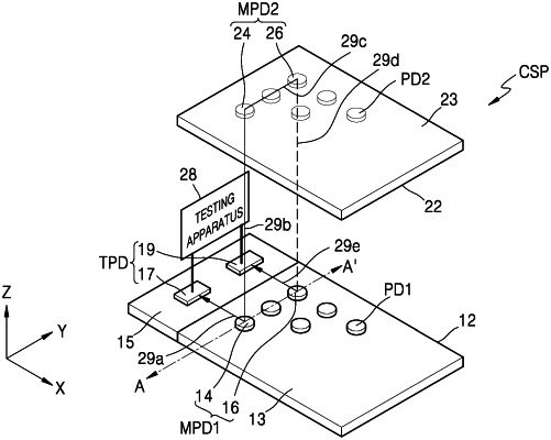
1. A method of manufacturing a chip-stacked semiconductor package, the method comprising:
providing a first chip including a first detection pad, a second detection pad, a first test terminal and a second test terminal, the first test terminal electrically connected to the first detection pad and the second test terminal electrically connected to the second detection pad;
stacking a second chip on the first chip with a gap therebetween, wherein the second chip includes a third detection pad facing the first detection pad and a fourth detection pad facing the second detection pad;
arranging the third detection pad to overlap the first detection pad and connecting the first detection pad with the third detection pad through a first medium;
providing a second medium between the fourth detection pad and the second detection pad, the second medium being different from the first medium; and
electrically connecting the fourth detection pad to the third detection pad via a conductive line; and
measuring a capacitance between the second detection pad and the fourth detection pad by using the first test terminal and the second test terminal.
|