| CPC H01L 22/32 (2013.01) [H01L 25/167 (2013.01); H01L 29/866 (2013.01); H01L 33/42 (2013.01); H01L 33/52 (2013.01); H01L 33/62 (2013.01); H01L 33/64 (2013.01)] | 15 Claims |
|
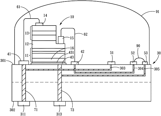
1. A vertical light emitting diode chip package with an electrical detection device, comprising:
a light emitting diode chip, provided with a chip conductive structure,
a lateral extending interface structure,
a semiconductor epitaxial structure,
an N-type electrode and a P-type bypass detection electrode, wherein the chip conductive structure is provided with a P-type main electrode located at a lower side, the lateral extending interface structure is arranged at one side, away from the P-type electrode, of the chip conductive structure; the semiconductor epitaxial structure and the P-type bypass detection electrode are arranged on an upper plane of the lateral extending interface structure; the semiconductor epitaxial structure and the chip conductive structure achieve an Ohmic contact by virtue of the lateral extending interface structure; and the N-type electrode is arranged at one side, away from the chip conductive structure, of the semiconductor epitaxial structure; and the chip conductive structure is provided with a structural metal layer, an alternative substrate adhesive layer and a high thermal conductive alternative substrate; wherein the structural metal layer is located below the lateral extending interface structure; the high thermal conductive alternative substrate is bonded with the alternative substrate adhesive layer below the structural metal layer; and the P-type main electrode is arranged below the high thermal conductive alternative substrate; and
a package substrate, provided with an upper plane and a lower plane, the lower plane of the package substrate being provided with,
an anode and a cathode thereon, the upper plane of the package substrate being provided with
a main first electrode,
a main second electrode,
a main third electrode,
a first electrical test contact, a second electrical test contact and a third electrical test contact thereon; wherein the N-type electrode is electrically connected with the main first electrode by a first chip bonding wire, the P-type bypass detection electrode is electrically connected with the main second electrode by a second chip bonding wire, the P-type main electrode is electrically connected by directly bonding the main third electrode through a chip-substrate bonding adhesive layer, the first electrical test contact is electrically connected with the main first electrode and the cathode, the second electrical test contact is electrically connected with the main second electrode, and the third electrical test contact is electrically connected with the main third electrode and the anode.
|