| CPC H01L 22/32 (2013.01) [H01L 25/0753 (2013.01); H01L 25/167 (2013.01); H01L 29/866 (2013.01); H01L 33/52 (2013.01); H01L 33/62 (2013.01)] | 19 Claims |
|
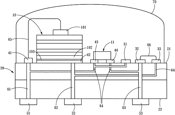
1. An LED package with multiple test pads and a parallel element which is used for chip bonding of a main element of LED chip and a parallel circuit secondary element, comprising:
a package substrate, wherein the package substrate is provided with an upper element plane and a lower SMD electrode plane located on two sides, the upper element plane is provided with a first electrode of the main element, a second electrode of the main element, a first electrode of the secondary element, and a second electrode of the secondary element, the first electrode of the main element and the second electrode of the main element are used for chip bonding of the main element of LED chip, the first electrode of the secondary element and the second electrode of the secondary element are used for chip bonding of the parallel circuit secondary element, and the first electrode of the main element is in electrical communication with the first electrode of the secondary element;
a first electrical test contact, wherein the first electrical test contact is disposed on the package substrate and electrically connected to the first electrode of the main element and the first electrode of the secondary element;
a second electrical test contact, wherein the second electrical test contact is disposed on the package substrate and electrically connected to the second electrode of the secondary element; and
a third electrical test contact, wherein the third electrical test contact is disposed on the package substrate and electrically connected to the second electrode of the main element.
|