| CPC H01L 21/76897 (2013.01) [H01L 21/7681 (2013.01); H01L 21/76849 (2013.01); H01L 21/76861 (2013.01); H01L 21/76879 (2013.01); H01L 23/5226 (2013.01); H01L 21/76816 (2013.01)] | 6 Claims |
|
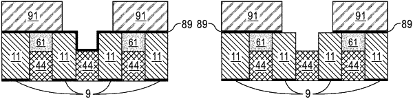
1. A method of forming a back end of line semiconductor wiring structure, the method comprising:
forming a plurality of first metal lines in a first dielectric material using a dual damascene process;
recessing the plurality of metal lines using a wet etching process;
depositing a second dielectric material above the plurality of first metal lines;
selectively removing a portion of the second dielectric material above at least one line of the plurality of first metal lines;
depositing an etch stop material over exposed surfaces of the first dielectric material, the second dielectric material, and the at least one line of the plurality of first metal lines;
depositing a third dielectric material over the etch stop material;
selectively removing a portion of the third dielectric material above the at least one line of the plurality of first metal lines;
selectively removing a portion of the etch stop material above the at least one line of the plurality of first metal lines; and
depositing a second metal material over the exposed surfaces of the first dielectric material, the second dielectric material, and the at least one line of the plurality of first metal lines.
|