| CPC H01L 21/76885 (2013.01) [H01L 21/76832 (2013.01); H01L 21/76837 (2013.01); H01L 23/5226 (2013.01)] | 14 Claims |
|
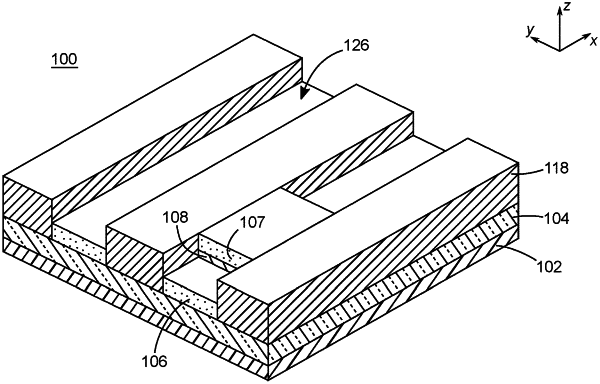
1. A method of forming an electronic device, the method comprising:
forming a first metallization line, the first metallization line having a first width;
forming an oversized via mask on a via metallization layer on the first metallization line, the oversized via mask having a mask width and a mask length, the via mask comprising an extreme ultraviolet (EUV) trilayer on a hard mask layer and the mask width greater than the first width of the first metallization line;
forming a via, the via having a via metal length that is equal to the mask width and having a via metal width that is equal to the first width; and
forming a second metallization line.
|