| CPC H01L 21/76877 (2013.01) [H01L 21/02068 (2013.01); H01L 21/76831 (2013.01)] | 16 Claims |
|
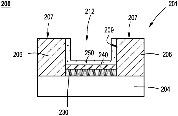
1. A method of forming a semiconductor structure, the method comprising:
cleaning a substrate to form a substrate surface substantially free of oxide, the substrate including at least one feature having a bottom surface and a sidewall surface, the bottom surface comprising silicon germanium (SiGe), and the sidewall surface comprising a dielectric material;
exposing the substrate surface to a first molybdenum precursor;
exposing the substrate surface to a reactant to selectively deposit a first molybdenum film on the bottom surface; and
forming a cap layer on the first molybdenum film or treating the first molybdenum film to form the cap layer, the cap layer comprising a metal nitride, a PVD metal, or combinations thereof,
the method performed in a processing chamber without breaking vacuum.
|