| CPC H01L 21/76802 (2013.01) [G11C 5/025 (2013.01); H01L 21/308 (2013.01); H01L 28/60 (2013.01); H10B 12/03 (2023.02); H10B 12/30 (2023.02)] | 11 Claims |
|
1. A method for preparing a semiconductor device, comprising:
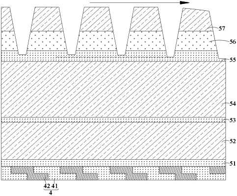
providing a wafer on which a semiconductor structure is formed;
forming a stacked film layer structure on a side of the semiconductor structure away from the wafer, a film layer in the stacked film layer structure farthest from the semiconductor structure being a first film layer;
reducing a thickness of the first film layer so that the thickness of the first film layer at where orthographic projection of the first film layer on the wafer locates at an edge of the wafer is less than the thickness of the first film layer at where orthographic projection of the first film layer on the wafer locates in middle of the wafer; and
patterning the stacked film layer structure to form through holes which communicate to the semiconductor structure.
|