| CPC H01L 21/76232 (2013.01) [H01L 21/02236 (2013.01); H01L 21/31155 (2013.01)] | 10 Claims |
|
1. A method of forming a semiconductor structure, comprising:
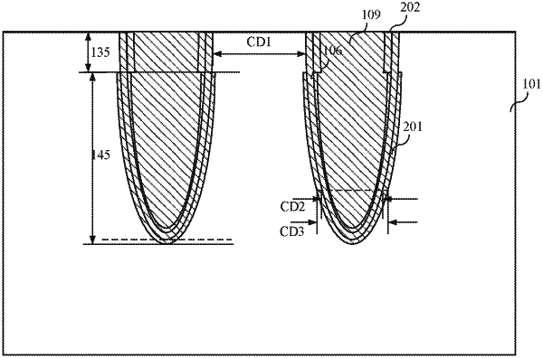
providing a semiconductor substrate, wherein a plurality of isolation grooves distributed at intervals are provided in the semiconductor substrate, each of the isolation grooves comprises a top region isolation groove and a bottom region isolation groove, and the top region isolation groove is at a higher position than the bottom region isolation groove;
forming a first protective layer covering a side wall of the top region isolation groove and a top of the semiconductor substrate;
performing oxidation treatment on the bottom region isolation groove to oxidize a part of the semiconductor substrate close to the bottom region isolation groove to form a second substrate isolation layer; and
forming a dielectric layer filling each of the isolation grooves, and etching the first protective layer and the dielectric layer higher than the top of the semiconductor substrate to form an isolation structure,
wherein the forming the first protective layer covering the side wall of the top region isolation groove and the top of the semiconductor substrate comprises:
forming a first protective film covering the top of the semiconductor substrate and a side wall of each of the isolation grooves;
forming a sacrificial layer filling the bottom region isolation groove;
treating the first protective film on the top of the semiconductor substrate and the side wall of the top region isolation groove to form the first protective layer; and
removing the sacrificial layer and the first protective film which is not subjected to the treating, wherein an etching rate of the first protective layer is less than an etching rate of the first protective film.
|