| CPC H01L 21/76 (2013.01) [H01L 21/2658 (2013.01); H01L 21/26533 (2013.01); H01L 21/76224 (2013.01); H01L 29/0642 (2013.01); H01L 29/1054 (2013.01); H01L 29/66651 (2013.01); H01L 29/7834 (2013.01)] | 20 Claims |

|
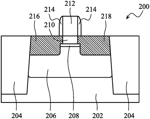
1. A device comprising:
a substrate having a shallow trench isolation feature (STI) disposed around a well in the substrate, wherein the well includes a first dopant and the STI has a top surface opposite the substrate that extends along a first plane, wherein the well includes an edge that faces the STI;
a source/drain feature disposed over the well and in direct contact with the edge of the well that faces the STI;
a channel disposed over the well adjacent the source/drain feature such that the channel does not extend above the first plane, wherein the channel includes a second dopant;
a gate electrode disposed over the channel; and
a barrier layer disposed between the channel and the well, wherein the barrier layer has a bottom surface facing the substrate and an opposing top surface facing away from the substrate, and wherein the source/drain feature directly contacts the top surface of the barrier layer.
|