| CPC H01L 21/67271 (2013.01) [G06N 5/04 (2013.01); G06N 20/00 (2019.01)] | 25 Claims |
|
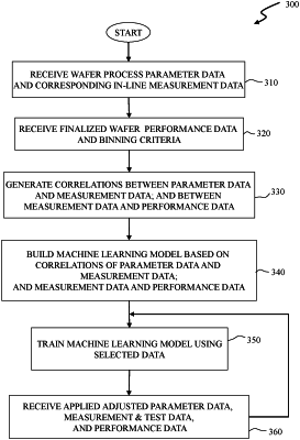
1. A method for generating a machine learning model for improving performance levels of semiconductor devices during fabrication, the method comprising:
determining, by one or more processors, a first set of correlations between process parameters applied to a metallization layer process of semiconductor device fabrication and data from measurement and test operations performed subsequent to the metallization layer of the semiconductor devices, for a plurality of metallization layers performed during fabrication of a plurality of semiconductor devices;
determining, by one or more processors, a second set of correlations between the data from measurement and test operations performed subsequent to the metallization layer of the semiconductor devices and predicted performance level of the semiconductor devices;
generating a machine learning model, based on the first set of correlations and the second set of correlations; and
training the machine learning model to:
determine an initial sorting bin, a target soring bin, and a current sorting bin of a first semiconductor device, and
determine adjustments to process parameters of a subsequent metallization layer that improve the performance levels of the first semiconductor device by compensating for performance-reducing conditions detected by prior process measurement and testing operations.
|