| CPC H01L 21/568 (2013.01) [H01L 23/3128 (2013.01); H01L 24/19 (2013.01); H01L 2224/12105 (2013.01); H01L 2224/32225 (2013.01)] | 21 Claims |
|
1. An apparatus comprising:
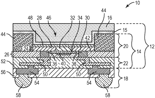
a mold device die comprising a device region, a thermally conductive film, and a first mold compound, wherein:
the device region includes a front-end-of-line (FEOL) portion and a back-end-of-line (BEOL) portion underneath the FEOL portion, wherein:
the FEOL portion comprises an active layer and isolation sections, which surround the active layer and extend vertically beyond a top surface of the active layer to define an opening within the isolation sections and over the active layer, wherein the isolation sections are formed of silicon dioxide; and
each of the isolation sections does not cover the top surface of the active layer;
the thermally conductive film resides at least over the top surface of the active layer of the FEOL portion within the opening, wherein the thermally conductive film has a thermal conductivity greater than 10 W/m·K and an electrical resistivity greater than 1E5 Ohm-cm; and
the first mold compound resides over the thermally conductive film, wherein:
silicon crystal, which has no germanium, nitrogen, or oxygen content, does not exist between the first mold compound and the active layer; and
a multilayer redistribution structure formed underneath the BEOL portion of the mold device die, wherein the multilayer redistribution structure comprises a plurality of bump structures, which are on a bottom surface of the multilayer redistribution structure and electrically coupled to the FEOL portion of the mold device die.
|