| CPC H01L 21/28052 (2013.01) [H01L 21/2855 (2013.01); H01L 21/28079 (2013.01); H01L 21/823443 (2013.01)] | 12 Claims |
|
1. A semiconductor device comprising:
a semiconductor body;
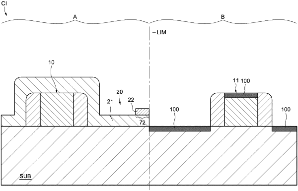
a first gate structure overlying a surface of the semiconductor body, the first gate structure being silicided;
a second gate structure overlying the surface of the semiconductor body, the second gate structure not being silicided;
an oxide layer overlying the second gate structure and extending toward the first gate structure; and
a silicon nitride region laterally spaced from the second gate structure and overlying a portion of the oxide layer between the first gate structure and the second gate structure, wherein the silicon nitride region occupies a surface area of less than 50% of a total surface area of the semiconductor body.
|