| CPC H01L 21/0337 (2013.01) [C23C 16/401 (2013.01); C23C 16/403 (2013.01); C23C 16/45536 (2013.01); C23C 16/45544 (2013.01); H01L 21/0228 (2013.01); H01L 21/0273 (2013.01); H01L 21/02115 (2013.01); H01L 21/02164 (2013.01); H01L 21/02178 (2013.01); H01L 21/02274 (2013.01); H01L 21/0332 (2013.01); H01L 21/0338 (2013.01); H01L 21/3081 (2013.01); H01L 21/3086 (2013.01); H01L 21/3088 (2013.01); H01L 21/30604 (2013.01); H01L 21/31058 (2013.01); H01L 21/31122 (2013.01); H01L 21/31144 (2013.01); C23F 1/08 (2013.01); H01L 21/67069 (2013.01)] | 20 Claims |
|
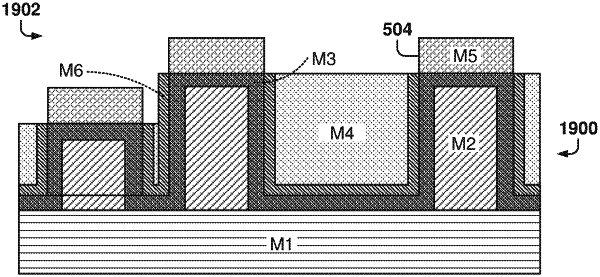
1. A method comprising:
adding a photo-resist material (M2) on top of a base material (M1) of a substrate, M2 defining a pattern for etching M1 in areas where M2 is not present above M1;
conformally capping the substrate with an oxide material (M3) after adding M2;
depositing a layer of a conformal material (M6) after conformally capping the substrate;
gap filling the substrate with filling material M4 after depositing M6;
removing top surfaces of M6 from the substrate after the gap filling;
selectively growing stop-etch material (M5) on exposed surfaces of M3;
removing M4 from the substrate after selectively growing M5; and
etching the substrate after removing M4 to transfer the pattern into M1.
|