| CPC H01L 28/20 (2013.01) [G01K 7/16 (2013.01); G01K 7/22 (2013.01); G01K 7/223 (2013.01); G01K 7/226 (2013.01); H01L 21/28035 (2013.01); H01L 23/34 (2013.01); H01L 27/0629 (2013.01); H01L 29/4916 (2013.01); G01K 7/01 (2013.01)] | 8 Claims |
|
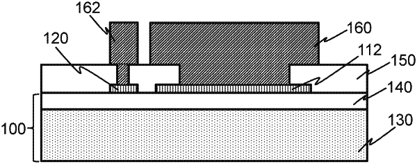
1. A semiconductor device comprising:
a device cell including a gate component configured to receive a gate control signal;
a temperature sensing component adjacent to the device cell;
a metal layer contacting a portion of the temperature sensing component; and
an interlayer dielectric layer covering at least partially the temperature sensing component and the gate component,
wherein each of the temperature sensing component and the gate component includes polycrystalline silicon,
wherein the temperature sensing component is formed as a polycrystalline silicon resistor,
wherein the temperature sensing component and the gate component are formed from a same polycrystalline silicon layer and spaced from each other;
wherein the temperature sensing component and the gate component are disposed on a common layer, and both the temperature sensing component and the gate component directly contact the common layer, the common layer being a dielectric layer;
wherein the polycrystalline silicon of the temperature sensing component is doped with N-type impurities of a first impurity concentration and the polycrystalline silicon of the gate component is doped with N-type impurities of a second impurity concentration, and the first impurity concentration is smaller than the second impurity concentration,
wherein the portions of the temperature sensing component contacting the metal layer are doped more heavily compared with other portions of the temperature sensing component,
wherein the temperature sensing component has a negative temperature coefficient, and
wherein the semiconductor device is selected From a group consisting of a metal-oxide-semiconductor field-effect transistor, an insulated-gate bipolar transistor, and a junction gate field-effect transistor.
|