| CPC H01L 27/1463 (2013.01) [H01L 21/02057 (2013.01); H01L 21/30604 (2013.01); H01L 27/1469 (2013.01); H01L 27/14634 (2013.01); H01L 27/14683 (2013.01); H01L 27/14698 (2013.01); H01L 27/1464 (2013.01); H01L 27/14636 (2013.01)] | 20 Claims |

|
1. A method of forming an image sensor, comprising:
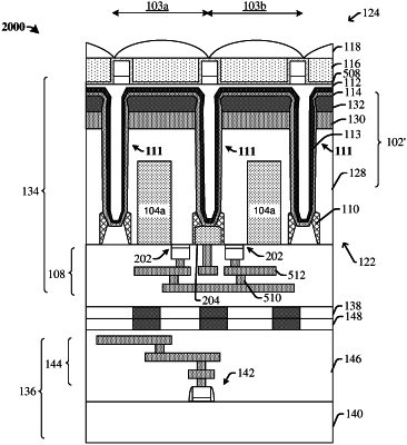
forming a plurality of photodiodes for a plurality of pixel regions from a front-side of an image sensing die, wherein a photodiode is formed to have a photodiode doping column with a first doping type surrounded by a photodiode doping layer with a second doping type that is different than the first doping type;
forming a deep trench between adjacent pixel regions in the photodiode doping layer from a back-side of the image sensing die, wherein an upper portion of the photodiode doping layer exposed to the deep trench is converted to a defective layer during the forming of the deep trench;
performing a cyclic cleaning process of at least two different etchants alternatively to remove the defective layer;
forming a doped liner precursor with the second doping type lining a sidewall surface of the deep trench, the doped liner precursor having a thickness smaller than 10 nm and a doping concentration greater than 1×1019cm−3;
forming a doped liner by performing an annealing process to facilitate dopant diffusion from the doped liner precursor to an adjoining portion of the photodiode doping layer; and
forming a dielectric fill layer filling an inner space of the deep trench to form a back-side deep trench isolation (BDTI) structure;
wherein the doped liner is formed with a surface dopant concentration greater than 1×1020cm−3 and a depth of 20 nm at which the dopant concentration is reduced to around 1015cm−3.
|