| CPC H01J 37/32045 (2013.01) [H01J 37/32027 (2013.01); H01L 21/3065 (2013.01); H01J 2237/3341 (2013.01)] | 29 Claims |
|
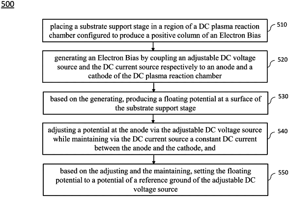
1. A method for atomic layer etching of a substrate, the method comprising:
generating a volume of gaseous plasma including diluent species, reactive species, and electrons of a uniform steady state composition in a positive column of a DC plasma proximate a substrate, thereby developing a floating potential at a surface of the substrate;
adjusting the floating potential to a known reference potential;
forming a corrosion layer on the substrate, the corrosion layer comprising corrosion layer species formed by adsorption of the reactive species to atoms of an atomic layer at the surface of the substrate;
applying a positive biasing potential to the substrate that is positive with respect to the floating potential;
based on the applying, drawing electrons from the volume of gaseous plasma to the surface of the substrate and imparting an energy level to drawn electrons for stimulating electron transitions in the corrosion layer species; and
based on the stimulating, desorbing the corrosion layer species, thereby etching away the atomic layer.
|