| CPC G11C 7/08 (2013.01) [G11C 7/12 (2013.01)] | 14 Claims |
|
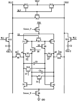
1. A sense amplifier, comprising:
an amplification circuit, configured to read data of a memory cell on a first bit line or a second bit line; and
a first offset voltage storage cell and a second offset voltage storage cell, respectively and electrically connected to the amplification circuit,
wherein in a case where the data in the memory cell on the first bit line is read, in an offset elimination stage of the sense amplifier, the sense amplifier is configured to store an offset voltage of the sense amplifier in the first offset voltage storage cell; and in a case where the data in the memory cell on the second bit line is read, in the offset elimination stage of the sense amplifier, the sense amplifier is configured to store the offset voltage of the sense amplifier in the second offset voltage storage cell,
wherein the amplification circuit comprises:
a first Positive channel Metal Oxide Semiconductor (PMOS) transistor;
a second PMOS transistor, a source of the second PMOS transistor being connected to a source of the first PMOS transistor;
a first Negative channel Metal Oxide Semiconductor (NMOS) transistor, a drain of the first NMOS transistor being connected to a drain of the first PMOS transistor; and
a second NMOS transistor, a drain of the second NMOS transistor being connected to a drain of the second PMOS transistor, and a source of the second NMOS transistor being connected to a source of the first NMOS transistor,
wherein a first end of the first offset voltage storage cell is connected to the drain of the first NMOS transistor, and a second end of the first offset voltage storage cell is connected to a gate of the second NMOS transistor,
wherein a first end of the second offset voltage storage cell is connected to a gate of the first NMOS transistor, and a second end of the second offset voltage storage cell is connected to the drain of the second NMOS transistor, and
wherein in the offset elimination stage of the sense amplifier, the first PMOS transistor and the second PMOS transistor are configured as a current mirror, and the first NMOS transistor and the second NMOS transistor are both configured to be in a diode connection mode.
|