| CPC G11C 29/12 (2013.01) [G11C 11/402 (2013.01)] | 8 Claims |
|
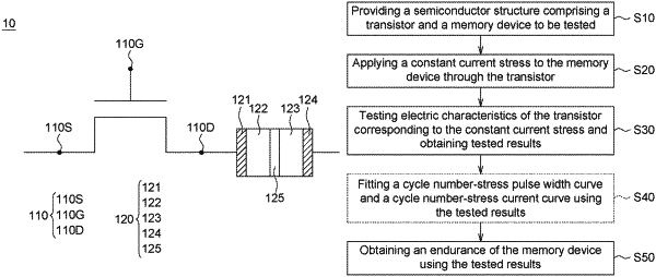
1. An endurance test method, the endurance test method using a semiconductor structure comprising a memory device to be tested, the endurance test method comprising:
providing the semiconductor structure, the semiconductor structure comprising a transistor and the memory device, wherein the transistor comprises a source, a drain, and a gate, the memory device is disposed at a drain side of the transistor and coupled to the drain, the memory device comprises a first electrode, a switch layer, a phase change memory layer, and a second electrode disposed sequentially, and the first electrode is coupled to the drain;
applying a constant current stress to the memory device through the transistor, wherein the constant current stress comprises at least one cycle each including a pulse;
testing electric characteristics of the memory device corresponding to the constant current stress and obtaining tested results; and
obtaining endurance of the memory device using the tested results;
wherein the tested results including a relation between the number of the at least one cycle and a stress pulse width of the pulse;
wherein the memory device further comprises a barrier layer between the switch layer and the phase change memory layer, and the barrier layer is formed of carbon.
|